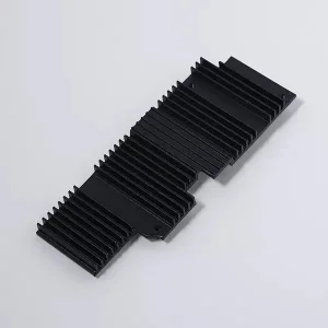
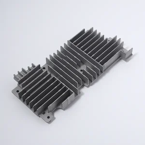
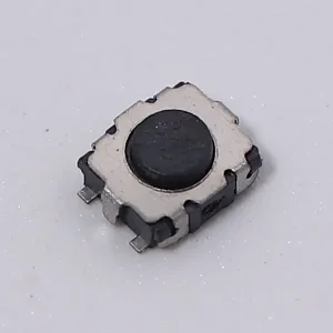
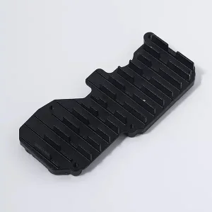
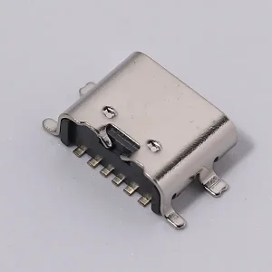
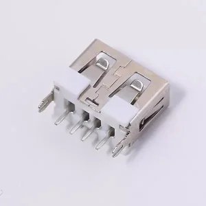
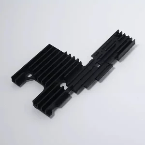
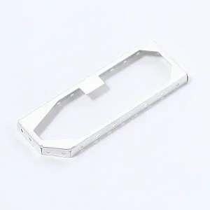
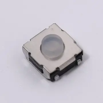
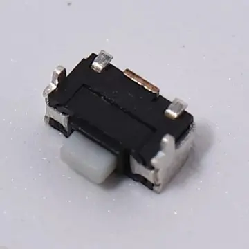
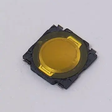
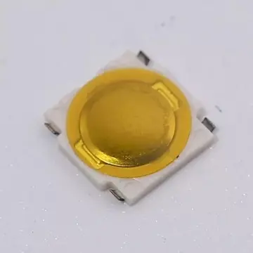
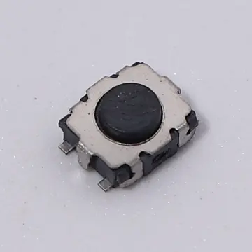
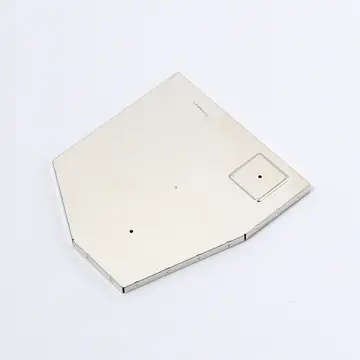
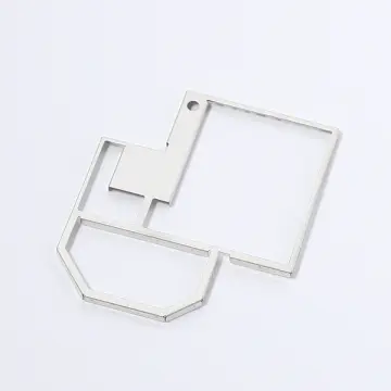
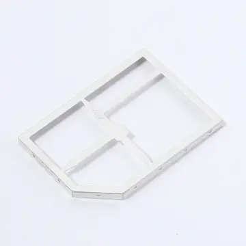
Founded in 2005, Wenzhou Stpete Electronics Technology Co., Ltd. has evolved into a leading high-tech enterprise at the forefront of the electronic components and RF shielding industry. We specialize in the end-to-end development, precision production, and global sales of board-level electronic components. Our diverse portfolio integrates high-frequency connectors, RF terminals, tactile switches, and high-performance electromagnetic compatibility (EMC) shielding frames.
Over two decades, we have solidified our authority in precision hardware design, collaborating directly with Tier-1 technological giants including Huawei and Hisense to engineer robust, high-frequency hardware systems. From raw material sourcing to structural stamping simulation, Stpete Electronics delivers high-yield production, ensuring maximum reliability and minimal signal degradation under the most rigorous operating conditions.

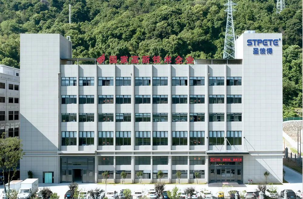
For Stpete, quality is a core standard. We are certified under ISO 9001, ISO 14001, and ISO 45001 (formerly OHSAS 18001). Our manufacturing facility in Wenzhou leverages automated production lines and advanced material testing infrastructure to supply the global electronics supply chain.
Our production floor features precision progressive stamping dies, high-speed press systems, and integrated insert molding cells. We perform extensive structural simulations (FEA and EMI modeling) to predict physical stresses and attenuation parameters before hard tooling begins. From material entry inspection through the optical measurement processes of final quality control, each process maintains tight mechanical tolerances of ±0.01mm to ensure flat, warp-free solder surfaces during SMT reflow.
Chinese precision metal manufacturers offer advanced technical capability, raw material integration, and high supply chain adaptability.
Our facility is positioned in Wenzhou's industrial hardware cluster, providing direct access to specialized surface plating, material testing, and base metal processing. This integration lowers logistics overhead and cuts prototyping lead times to as short as 7 days.
We design, build, and maintain our progressive dies in-house. Running stamping speeds up to 600 strokes per minute, our dies include automated features like micro-dimple forming and pre-cut release tabs to optimize the output of multi-cavity shielding frames.
Every production run undergoes AOI (Automated Optical Inspection), X-ray coating thickness verification, and solderability testing. We control coplanarity to within 0.08mm, eliminating pick-and-place errors and cold solder joints during high-speed SMT assembly.
Selecting the correct base alloy is critical to achieving target electromagnetic attenuation, mechanical durability, and electrical contact resistance. The table below details the properties of materials used for shielding frames:
| Material Type | Shielding Range (EMI/RFI) | Solderability Performance | Oxidation & Corrosion Resistance | Common Applications |
|---|---|---|---|---|
| Nickel Silver (C5210/C5191) | Excellent (10MHz - 40GHz) | Excellent (Directly solderable, no plating required) | Outstanding (Creates a stable, self-passivating oxide) | Smartphones, Automotive Radar, 5G RF Transceivers |
| Pre-Tin Plated Cold Rolled Steel | Good (Low to High Frequencies) | Very Good (Pre-tin coating supports SMT reflow) | Moderate (Edges require sealing post-stamping) | Smart Meters, IoT Modules, Set-Top Boxes |
| Phosphor Bronze (with Sn Plating) | Excellent (Mid to High Frequencies) | Excellent (Post-plated tin is highly solder-compatible) | Good (Protective tin layer prevents copper oxidation) | Telecom Routers, Optical Transceiver Shells |
| Stainless Steel (SUS 304) | Fair to Good (High structural rigidity) | Difficult (Requires specialized acid flux or selective plating) | Outstanding (Impervious to atmospheric corrosion) | Rugged Military Equipment, High-Vibration Automotive ECU |
As boards grow denser and frequencies rise, shielding hardware must evolve. The following shifts define the future of precision board-level shielding:
Modern components require shielding heights below 0.8mm. Using thin-gauge alloys (down to 0.10mm) and custom micro-draw dies, Stpete manufactures low-profile frames that protect RF components while staying within standard z-height profiles.
Instead of placing multiple shielding cans, engineers now use single multi-cavity frames. Stpete builds segmented frames that isolate RF front-ends, digital processors, and power management units under one cover, reducing board area and assembly time.
Shielding frames can trap heat from high-speed silicon. Stpete integrates customizable patterns of ventilation holes and thermal interface pads on top of shielding lids, creating a path to dissipate heat without compromising EMI attenuation.
Global procurement teams look for more than stamping capacity; they require reliable quality, clear logistics, and collaborative engineering. Our technical support team works directly with client engineering departments during early design stages, offering DFM (Design for Manufacturability) analysis to optimize draft angles, bend radii, and material utilization.
To support high-speed SMT assembly lines, Stpete packs shielding components in robust carrier tapes (Tape-and-Reel packaging) designed to EIA-481 standards. This ensures precise pickup by SMT vacuum nozzles, preventing physical deformation during high-speed assembly. We coordinate closely with global shipping partners to deliver components safely and on schedule, minimizing logistics risk for global production facilities.
Beyond automation and machinery, our organizational culture emphasizes collaboration and professional alignment. Team-building exercises and cross-departmental training programs keep our production engineers, quality assurance auditors, and customer service teams aligned to support client requirements.

Stpete custom-stamped shielding frames are engineered for demanding applications across several key industries:
Our shielding frames protect sensitive ADAS controllers, radar systems, and telematics control units (TCU) from power-train noise and external interference. They are designed to withstand thermal cycling and continuous mechanical vibration.
We supply segmented shielding systems that isolate RF power amplifiers from digital signal processors in 5G base stations. These designs feature ventilation apertures optimized for high-frequency attenuation.
To support compact IoT designs, we produce micro-scale shielding frames from pre-tin plated steel, providing cost-effective EMI protection for high-volume automated production lines.
Our products protect high-speed lines in USB Type-C and custom interconnect systems, preserving signal integrity from noise generated by nearby processors and screens.
Our dedicated engineering department leads our technological innovation. We invest over 15 million RMB annually in engineering research, maintaining a library of 21 active patents. Our team focuses on high-speed stamping mechanisms, micro-drawing techniques for low-profile components, and advanced plating methods.
This commitment to research allows us to provide engineering support during the initial stages of product development. By identifying and resolving potential production issues early, we help customers accelerate time-to-market while ensuring high quality standards.
In-depth answers to key technical questions about the design, materials, and manufacturing of precision board-level shielding:
Stpete utilizes integrated stamping, insert molding, finished assembly, and automated production technologies. Our factory continuously updates manufacturing systems to improve throughput and consistency for complex geometries.
By automating raw material feeding, part transfer, and downstream packaging, we minimize physical handling. This reduction in manual steps lowers contamination risk and helps maintain structural dimensions, ensuring board-level components arrive in optimal condition for automated pick-and-place lines.
 Stpete Electronics