Understanding the engineering mechanics and electromagnetism behind high-performance bent shielding covers.
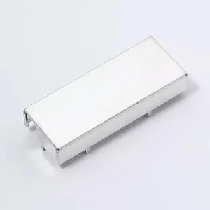
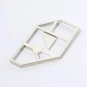
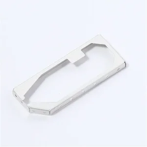
In modern electronic architecture, the dramatic increase in operational frequencies and the packing density of printed circuit boards (PCBs) have made Electromagnetic Interference (EMI) and Radio Frequency Interference (RFI) critical challenges. A Bent Shielding Cover, often referred to as an EMI shield can, is a metal protective enclosure designed to isolate delicate components from external radiated electromagnetic fields and prevent internal circuits from leaking noise to surrounding units. This is fundamental to ensuring electromagnetic compatibility (EMC) in electronic assemblies.
From a physical standpoint, a shielding cover operates on the principles of a Faraday Cage. When an electromagnetic wave encounters the metallic barrier of a bent shielding cover, two primary attenuation mechanisms occur:
For high-frequency applications like 5G, Wi-Fi 6E/7, and automotive radar (operating above 24GHz), designing bent shielding covers requires strict adherence to tight dimensional tolerances. Micro-gaps between the cover and the PCB ground plane can act as slot antennas, allowing high-frequency harmonics to escape. Thus, maintaining absolute co-planarity, optimizing bend radii, and implementing strategic vent arrays are critical design constraints.
An authoritative analysis of metal alloys and precision stamping dynamics for bent shield manufacturing.
Selecting the optimal material for a bent shielding cover is a balance between shielding effectiveness (SE), solderability, weight, environmental corrosion resistance, and cost. Below are the primary industrial alloys utilized in precision stamping:
| Material Alloy | Shielding Effectiveness | Solderability | Key Advantage |
|---|---|---|---|
| Nickel Silver (C7521/C7701) | Excellent (Up to 80 dB) | Superb (No plating needed) | Corrosion resistance & ease of reflow soldering |
| Tin-Plated Steel (SPCC/SPTE) | High (Particularly Low-Freq) | Good | Highly cost-effective structural choice |
| Stainless Steel (SUS301/304) | Moderate-High | Poor (Requires post-plating) | High mechanical yield strength for frame parts |
| Phosphor Bronze (C5191) | Excellent Conductivity | Excellent (When plated) | Great spring properties for multi-cavity clips |
The manufacturing process of bent shielding covers relies heavily on progressive die stamping. Progressive die technology executes multiple operations—such as piercing, blanking, bending, and forming—sequentially within a single stroke of the stamping press. Because shielding covers are mounted directly onto PCBs via Surface Mount Technology (SMT), controlling the flatness of the mating surface is critical. Industrial standard tolerances require co-planarity within < 0.10mm (0.004 in) to prevent solder bridging or dry joints during reflow assembly.
Custom shield solutions engineered for demanding global industries and harsh environments.
In electric vehicles, heavy switching noise from high-voltage inverters poses a constant threat to sensitive sensor arrays. Custom-designed bent shielding covers protect Advanced Driver Assistance Systems (ADAS), LiDAR modules, and battery management controller PCBs from harsh electromagnetic transients.
Telecommunications hardware handles extreme data rates over millimeter-wave bands. Bent shield cans act as multi-cavity isolation boundaries, mitigating cross-talk between local oscillators, low-noise amplifiers (LNAs), and power amplifier blocks on high-density RF boards.
Smartphones, high-frequency routers, and wearable IoT sensors packing RF antennas (Bluetooth, Wi-Fi, GPS) into micro-footprints require thin-gauge (0.15mm to 0.20mm) shielding covers. They shield processors from adjacent RF transceiver radiation, maximizing signal clarity.
A premier Chinese high-tech manufacturer specializing in precision connectors and board-level shielding.

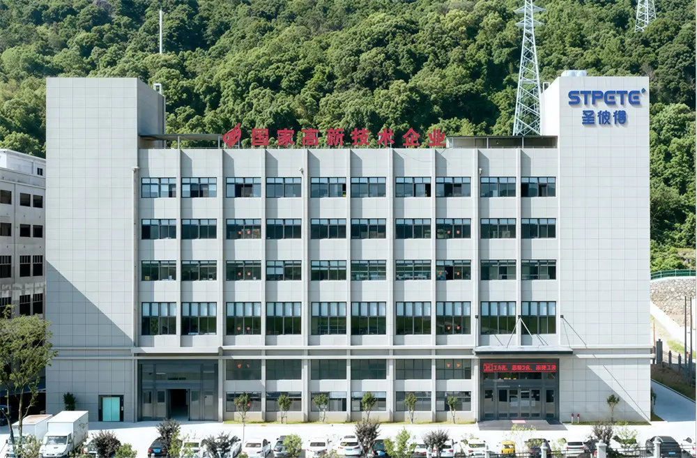
Established in 2005, Wenzhou Stpete Electronics Technology Co., Ltd. has evolved into a leading high-tech enterprise dedicated to the R&D, manufacturing, and international trade of precision electronic connectors and custom sheet-metal stamping components, including premium bent shielding covers. With almost two decades of technical evolution, we have established a solid reputation globally for superior product consistency and efficient client services.
Our core capabilities range from initial product development and prototype modeling to ultra-high-speed automated assembly. By combining in-house tooling manufacturing with advanced quality assurance protocols, we ensure every part delivered aligns with international dimensional and chemical regulations.
Why leading global OEMs choose Chinese manufacturers for precision bent shielding covers.
The global electronic manufacturing sector moves at a rapid pace, demanding faster time-to-market and seamless transitions from design to high-volume manufacturing. The Chinese metal stamping and connector supply chain offers unique advantages in cost-efficiency, technical capability, and speed:
Strict operational compliance, high-precision tooling, and validation methodologies.
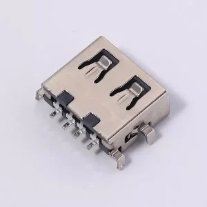
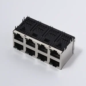
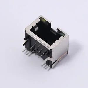
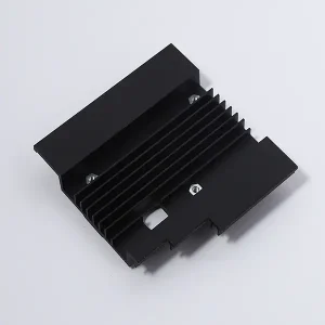
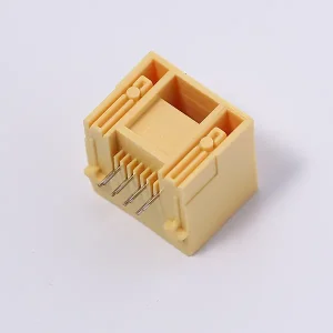
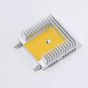
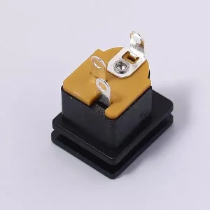
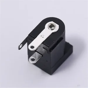
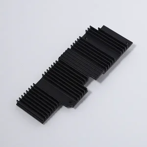
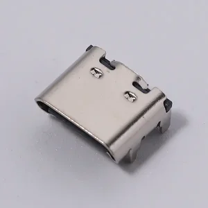
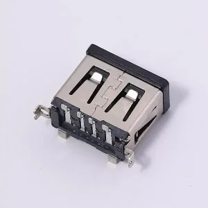
At Stpete, quality is guided by advanced technology and based on safety. From the initial selection of raw materials, to the production line processing, and finally to the inspection and testing process, every step is meticulous. We have a full set of equipment to produce IF Radio-Frequency Terminals, FCB Network Jacks, DC Power Outlets, USB Sockets, AV Pin Jack Boards, Radiators, and custom shielding brackets.
We operate high-level punching machines and CNC equipment to guarantee high accuracy and repeatability. Advanced testing inspection machines verify both incoming materials and finished goods. We implement multiple inspection checkpoints at every step of production to eliminate factory defects. Stpete is certified in ISO 9001, ISO 14001, ISO 45001 (formerly 18001 equivalent), and holds more than 21 research and development patents. We maintain a staff of 30+ technical R&D personnel, with an annual R&D investment exceeding 15 million Yuan, and collaborate with top brands like Huawei and Hisense.

To ensure co-planarity and defect-free output, we utilize automated 3D optical inspection systems on our progressive stamping lines. Real-time vision-based measurement devices inspect critical dimensions, including leg heights, flange angles, and co-planarity, down to the micron level. Any out-of-tolerance piece is detected and flagged, preventing manual sorting bottlenecks and reducing production waste.
Exploring the next frontier of electromagnetic compatibility (EMC) solutions.
As electronic systems grow more powerful and compact, shielding designs must evolve. Stpete is actively developing solutions to meet tomorrow's technical challenges:
A unified team committed to precision engineering excellence and collaborative customer service.
Behind our technical capabilities is a dedicated team of engineers, technicians, and customer specialists. This summer, our company organized an outdoor team-building activity to strengthen cohesion and foster teamwork. The event took place in a picturesque natural setting, providing a perfect backdrop for enhancing team spirit and collaboration.
The activity was designed to promote unity and cooperation among employees. Through a series of challenging and fun exercises, the participants had the opportunity to work together, communicate effectively, and problem-solve as a team. It was a great chance for everyone to bond, both personally and professionally, outside the confines of the office environment.
One of the highlights of the day was a series of team-based challenges that required trust, coordination, and quick thinking. These activities encouraged individuals to step out of their comfort zones, build trust in their colleagues, and see the value of working together towards a common goal. As a result, the event not only improved teamwork but also boosted morale and motivation within the company.
Furthermore, the outdoor setting provided a refreshing change of scenery, allowing everyone to unwind and connect with nature. This change of environment helped reduce work-related stress and promote a sense of well-being among the participants. It was a great opportunity for the team to relax, recharge, and return to work with renewed energy and enthusiasm.

Answers to common design and manufacturing questions for shielding covers.
For inquiries about our products, customization services, or pricelists, please leave us a message. Our technical support team will contact you within 24 hours to discuss your project requirements.
 Stpete Electronics