 Stpete Electronics
1 / 1
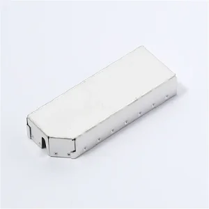
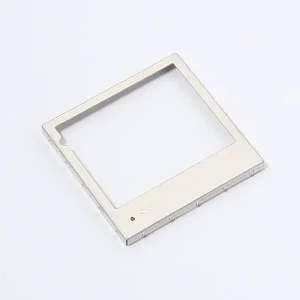
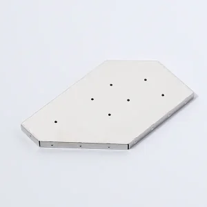
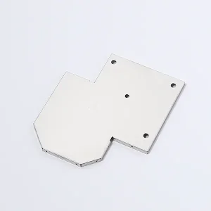
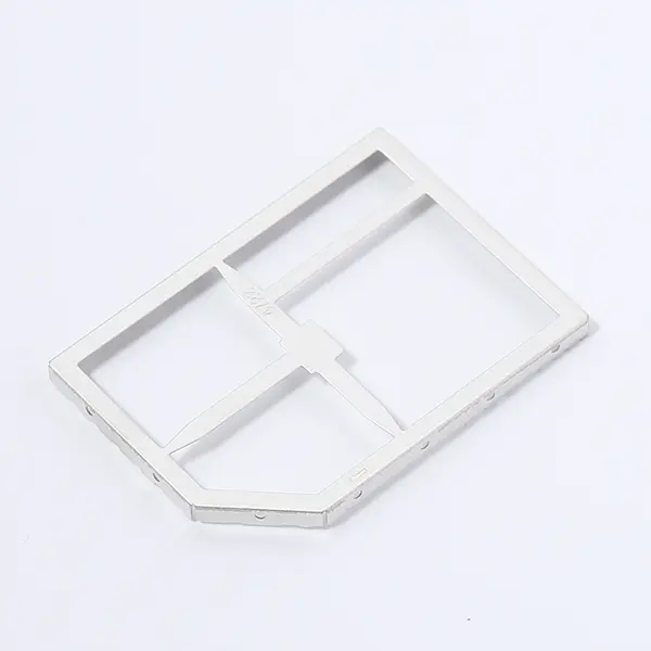
Crafted from high-quality tinplate, this shielding frame balances cost-effectiveness with exceptional performance: its inherent corrosion resistance and solderability ensure reliable long-term operation, while the lightweight yet rigid structure avoids adding unnecessary bulk to end products.
Unlike generic stamping parts, P-3650-K3 utilizes advanced precision bending and stamping integration technology, achieving tight dimensional tolerances (±0.05mm) and consistent shielding effectiveness across every unit, making it ideal for high-volume production lines.
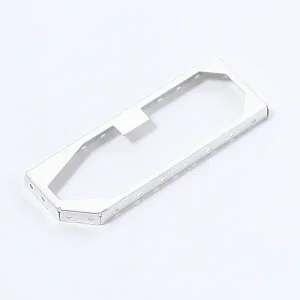
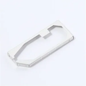
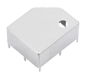
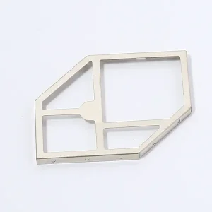
Its side-mounted through-hole design allows secure soldering directly onto PCBs, eliminating displacement risks during assembly or vibration-prone operating conditions. The hollow frame layout optimizes heat dissipation while blocking high-frequency EMI signals.
Clients can customize dimensions, plating finishes (tin, nickel, or gold), material thickness, and internal partition layouts to align with their unique PCB designs. Our in-house R&D team provides free technical consultation and rapid prototyping (3-7 days lead time).
The P-3650-K3 protects RF modules in 5G base stations, safeguards sensor circuits in automotive ADAS systems, shields control boards in industrial IoT gateways, and ensures signal purity in medical monitoring devices. Its versatility and reliability have made it a trusted choice for global electronics manufacturers seeking cost-efficient EMI solutions.
Contact us today to request samples, obtain detailed technical specifications, or discuss your Through-hole Shielding Frame requirements.
The frame is constructed from high-quality tinplate, which provides an optimal balance of cost-efficiency, mechanical strength, corrosion resistance, and excellent solderability for long-term performance.
The side-mounted through-hole design allows the frame to be securely soldered directly onto the PCB. This prevents displacement during assembly or in high-vibration environments, while the hollow layout promotes heat dissipation and mitigates component overheating.
Yes, we support flexible OEM customization. You can customize the dimensions, plating finishes (including tin, nickel, or gold), material thickness, and internal partition layouts to match your specific PCB layouts.
By utilizing advanced precision bending and stamping integration processes, we achieve a tight dimensional tolerance of ±0.05mm, ensuring high consistency for automated production lines.
It is widely used across various industries, including protecting RF modules in 5G base stations, safeguarding sensor circuits in automotive ADAS systems, shielding industrial IoT gateways, and protecting medical monitoring devices.
We offer rapid prototyping services with a lead time of 3 to 7 days, supported by our in-house R&D team to help speed up your product development cycle.