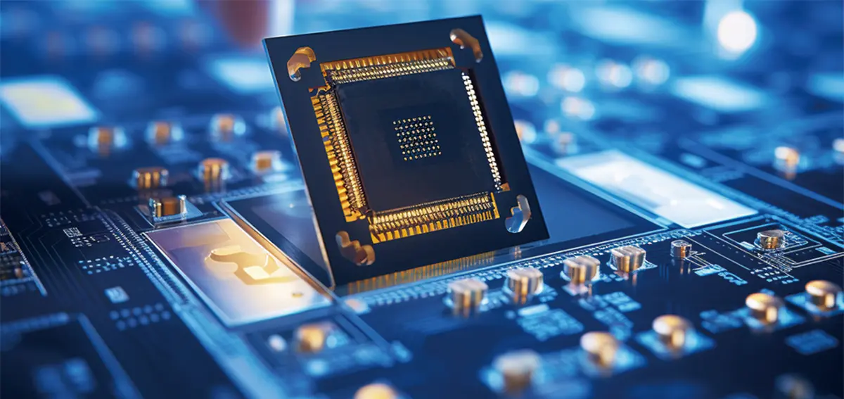
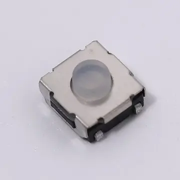
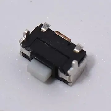
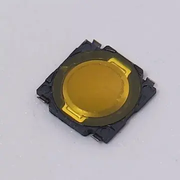
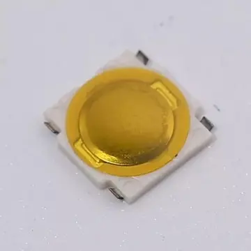
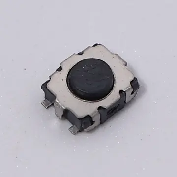
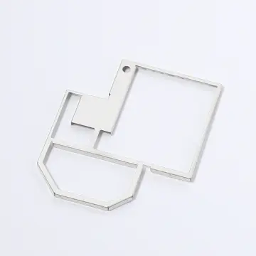
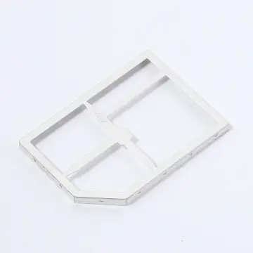
Premium grade hardware supporting global telecommunication infrastructures and data centers
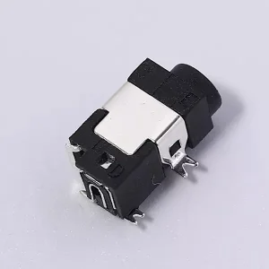
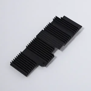
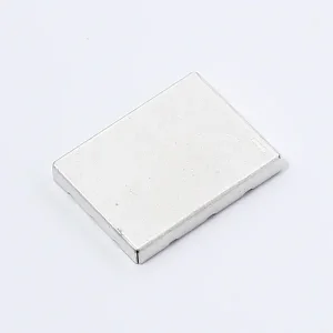
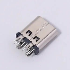
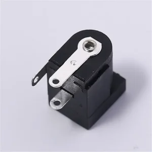
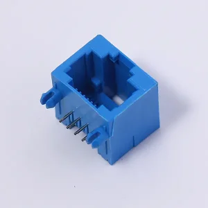
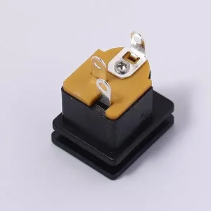
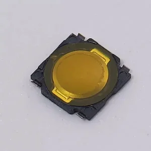
As data center architectures transition to 400G, 800G, and 1.6T speeds, the role of the custom optical module enclosure has evolved from basic mechanical protection to a core optoelectronic component. These advanced casings are critical to stabilizing optical pathways, managing extreme thermal limits, and eliminating electromagnetic interference (EMI) that can degrade signal integrity at high frequencies.
Whether dealing with standard pluggable formats like SFP-DD, QSFP-DD, OSFP, or emerging Co-Packaged Optics (CPO) architectures, high-precision machining tolerances are non-negotiable. Modern enclosures require dimensional precision within micron-level ranges to ensure absolute alignment between internal laser diodes, photodetectors, and complex fiber coupling arrays. A variation of even 5 microns can induce significant insertion loss, rendering high-speed transceivers inefficient.
Additionally, the internal mechanical configuration must act as a perfect Faraday cage. High-speed signal processing chips generate massive RF emissions. Without premium structural sealing—often achieved through specialized alloy formulation, precise CNC milling, and selective surface treatments like nickel or conductive tin plating—these transceivers fail global regulatory compliance standards such as FCC and CE certifications.


Established in 2005, Wenzhou Stpete Electronics Technology Co., Ltd. has dedicated two decades to developing and manufacturing high-precision electronic connectors and optoelectronic components. Our manufacturing facility represents the pinnacle of Chinese high-tech hardware integration.
Stpete operates under a robust quality system backed by ISO 9001, ISO 14001, and ISO 45001 certifications. We run automated insert molding, finished assembly, and precise stamping operations. Our R&D team consists of more than 30 technical specialists who hold over 21 research and development patents, allowing us to maintain a forward-looking technical pipeline.
We invest over 15 million CNY annually into direct R&D. This investment supports co-development and validation programs alongside leading global network infrastructure brands like Huawei and Hisense. This experience in Tier-1 supply chains guarantees that our engineering documentation, production control plans, and test methodologies align with the most rigorous global expectations.
A statistical showcase of Wenzhou Stpete's long-term infrastructure and commitment to high-precision hardware execution
How we control variables to deliver stable mechanical performance at scale
We implement specialized nickel-tin and zinc-nickel alloy platings to guarantee maximum shielding effectiveness up to 40 GHz. This effectively mitigates crosstalk in multi-channel optical systems.
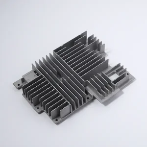
Integrating heat sinks directly into the enclosure chassis. Utilizing high-conductivity copper bases and specialized cooling fin arrays to support module thermal dissipation up to 30W.
Machined using multi-axis CNC machines to achieve critical dimensional tolerances down to ±0.005mm. This guarantees optimal latching mechanisms and minimizes mating wear cycles.
A closer look at the logistical, financial, and technical benefits of working with Chinese manufacturers
China’s Yangtze River Delta and Pearl River Delta harbor the world's most concentrated optical communications supply chain. At Wenzhou Stpete Electronics, we exploit this geographic cluster effect. Raw materials, precision mold tools, multi-axis die casting machinery, and electroplating lines are located within a small radius.
This proximity reduces lead times for complex custom prototypes from several weeks to just a few days. Our customers receive rapid design iterations, ensuring their time-to-market advantage in fast-moving industries like AI data centers.
High-speed network deployments demand scalability. Our manufacturing facility combines insert molding with automated precision assembly, allowing us to pivot from prototyping low-volume, high-complexity transceivers to managing multi-million-unit commercial rollouts.
By automating critical steps in our production lines, we reduce operator error, maintain high Cpk values (>1.67), and keep unit costs highly competitive without compromising structural quality.
Our incoming quality control (IQC) protocol analyzes every batch of raw material—whether zinc alloy, copper, or engineered plastics—using spectrophotometry and mechanical testing. This ensures that the material structural integrity is flawless.
This meticulous tracking ensures that our enclosures remain resistant to stress relaxation, high temperatures, and corrosion. This translates directly to a lifespan exceeding 15 years in rugged telecom environments.
For international enterprise buyers, regulatory compliance is a major hurdle. Stpete provides comprehensive documentation, including full REACH and RoHS declarations.
We perform regular trace testing on our plating systems to guarantee they are entirely lead-free and cadmium-free, meeting environmental mandates in the European Union, North America, and APAC regions.
Understanding the impact of AI infrastructure on optical module design
AI clusters require high-density interconnects. Enclosures must shrink in size while improving airflow dynamics and maximizing the surface area of external cooling fins.
Moving optical engines onto the silicon substrate shifts enclosure design from standard pluggable form factors to internal board-level hybrid shielding housings.
Next-generation chips generate substantial heat. Transceiver housings must operate reliably under continuous temperatures reaching up to 85°C without deformation.
Aligning manufacturing capabilities with Western standards for smooth integration
We maintain strict adherence to globally recognized quality management systems. Our raw materials are completely traceable, and our manufacturing plants comply with ISO certification frameworks to ensure safety and quality standards across all production runs.
A key component of our long-term reliability is our focus on team development and corporate culture. We actively host annual team-building initiatives to enhance cohesion, align cross-departmental communications, and encourage shared accountability.
This investment in our human capital reduces staff turnover and keeps our precision technicians focused on quality metrics. This collaborative internal environment translates directly to reliable, defect-free production lines and faster customer service response times for our global clients.

Insights into custom optical enclosure manufacturing, sourcing, and performance parameters
Zinc alloy (specifically Zamak 3 and Zamak 5) is the primary material choice due to its excellent die-casting properties, dimensional stability, and natural electromagnetic shielding. For components demanding high thermal performance, we often integrate copper or aluminum alloy heatsinks directly into the main zinc enclosure body.
We control EMI by optimizing physical sealing and applying custom surface treatments. Electroless nickel plating or tin-nickel plating is applied to internal cavity surfaces to guarantee a continuous conductive surface. Additionally, our design parameters ensure that the tolerances at mechanical joints are minimized to prevent RF leakage.
Yes. We specialize in custom configurations. Our R&D team can modify structural profiles, layout internal mounting locations, change heatsink fin heights, and adjust latch configurations to meet your specific PCB footprint and system airflow demands.
We use automated visual inspection systems (AOI), high-precision Coordinate Measuring Machines (CMM), and automated mechanical test jigs. We maintain a continuous SPC (Statistical Process Control) program on our CNC and stamping lines, ensuring Cpk values remain above 1.67 for critical alignment features.
Initial design reviews and tooling setup typically take 15 to 21 days depending on structural complexity. Once tooling is validated, we can produce pilot batches within 7 days. Standard mass-production runs are usually shipped within 30 days.
Yes. All materials, surface treatments, and electronic components we produce are fully compliant with RoHS and REACH regulations. We provide certificates of compliance and full chemical composition analyses with every batch order.
Premium solutions for telecommunications, computing, and high-frequency power distribution

 Stpete Electronics