Premium EMI Shielding components and frames designed for high-frequency signal integrity in industrial networks.
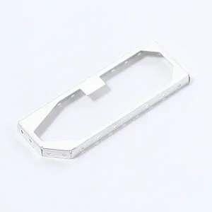
Ultra-precise metal enclosures featuring excellent coplanarity for automatic SMT lines in French technological hubs.
View Details →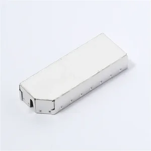
High attenuation shielding cans tailored for telecom devices, optimized for French industrial requirements.
View Details →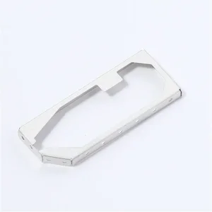
Custom multi-cavity board-level shielding frames for highly integrated complex PCB systems.
View Details →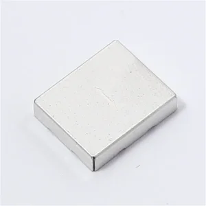
Heavy-duty nickel-silver RF shielding frames providing long-term solderability and corrosion resistance.
View Details →Paris and the wider Île-de-France region represent the epicenter of high-tech research, aerospace innovation, and automotive engineering in Continental Europe. With clusters like Paris-Saclay driving breakthroughs in deep tech, quantum computing, and autonomous mobility, the demand for highly reliable Electromagnetic Interference (EMI) and Radio Frequency Interference (RFI) shielding solutions has surged.
As electronic systems shrink and operate at higher frequencies (such as mmWave 5G and early-stage 6G components), shielding frames serve as the front line of defense against noise cross-talk. French manufacturing frameworks must conform to rigorous European Standards (EN) for Electromagnetic Compatibility (EMC), managed by regulatory bodies like the French National Frequency Agency (ANFR). Our high-precision shielding frames provide up to 80 dB of attenuation, safeguarding signal integrity in dense urban Parisian deployments, including railway control grids, telecom base stations, and smart IoT networks.
"Whether targeting aerospace telemetry in Paris-Saclay or connected smart grid deployments across France, our shielding frames deliver consistent thermal dissipation and absolute EMI protection."


Modern global logistics require balancing rapid engineering iterations with manufacturing cost efficiency. Our state-of-the-art production facility in Wenzhou, China, bridges this gap by integrating direct raw material sourcing, automated mold building, and high-speed progressive metal stamping.
Compared to European domestic prototyping, our vertically integrated plant allows French OEMs to reduce tooling lead times by up to 40% and tooling costs by up to 50%. We support diverse raw materials including Nickel-Silver (for superior corrosion resistance and weldability), Tin-plated Steel (for optimal economy), and Beryllium Copper (for high elasticity). Automated inline visual inspection systems check planar tolerance levels down to 0.05 mm, ensuring hassle-free processing on French SMT high-speed pick-and-place lines.
A trusted global supplier of advanced electronic connectors and RF/EMI shielding frames, established in 2005.
Wenzhou Stpete Electronics Technology Co., Ltd. has stood at the forefront of precision component manufacturing for over two decades. Specialized in the development, high-volume production, and worldwide sales of high-reliability electronic connectors and shieldings, we have cemented an exemplary reputation among top-tier enterprises in domestic and international markets, including partners like Huawei and Hisense.
Quality assurance is not a secondary checkbox for St. Peter—it is our guiding industrial philosophy. From early-stage alloy selection to automated stamping, deburring, and high-density tape-and-reel packaging, every process step undergoes rigorous quality control. Backed by certified management systems including ISO 9001, ISO 14001, and OHSAS 18001, we secure high repeatability and low defect rates, allowing French buyers to confidently integrate our components into mission-critical hardware.
Our production facilities feature high-speed precision stamping lines, advanced CNC mills, and wire-cut EDM equipment for rapid mold manufacturing. Beyond shielding frames, our product portfolio extends to IF radio-frequency terminals, FCB network jacks, DC power sockets, USB connectors, AV boards, and micro-radiators. With an annual R&D investment exceeding 15 million CNY and a team of 30+ dedicated technical engineers holding 21 patents, we tackle complex shielding geometry challenges, including multi-cavity designs with thermal integration features.

Our engineering prowess relies on a cohesive and highly motivated workforce. Stpete Electronics organizes quarterly outdoor team-building challenges and cross-departmental technical training sessions. These programs foster collaboration, open communication, and problem-solving skills under tight deadlines. We believe that this collaborative culture directly translates to better service, fast customer support responses, and reliable delivery for our procurement clients in France and worldwide.
Delivering high-precision electronic shielding frames from concept layout to high-volume assembly lines.
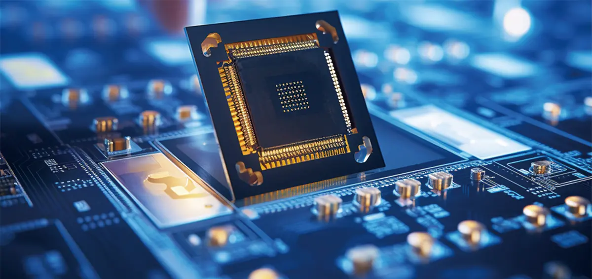
Our team of 30+ engineering specialists continually refines shielding designs, securing 21+ design patents to date, and ensuring compatibility with modern automated SMT assembly.

Quality is our bottom line. From initial raw material verification to coordinate measurement testing, our comprehensive quality control protocols ensure zero defects reach your assembly lines.

By combining in-house progressive tooling design with automated production machinery, we deliver consistent, cost-effective shielding solutions for large B2B orders.
Choosing the correct board-level shielding design is critical for B2B electronics manufacturers. An inadequate design can result in electromagnetic interference (EMI), leading to signal degradation or failing EMC certification tests. Here, we outline the primary technical guidelines and industry trends affecting the European market.
Design engineers must choose between one-piece and two-piece shielding configurations. One-piece shielding cans are soldered directly to the ground traces on the PCB, providing the most cost-effective and structurally rigid layout. However, they restrict access to components for rework. Two-piece shielding systems consist of a frame soldered to the board and a removable lid that clips securely into place. This design simplifies testing and rework during production and field servicing, and is widely used in high-value telecom and automotive assemblies in Paris and globally.
Material choices directly impact attenuation levels, weight, and assembly cost:
As components shrink, PCB assembly houses face challenges with frame warping during reflow soldering. If a frame's coplanarity exceeds 0.08–0.10 mm, it can lead to open joints or weak solder connections. Our progressive stamping processes keep coplanarity below 0.05 mm. Additionally, multi-cavity shielding frames can be designed with integrated vents or internal thermal pads to dissipate heat from processors, combining thermal management with EMI shielding.
Expert answers to common engineering, procurement, and shipping questions for French and global B2B clients.
Explore our catalog of certified shielding frames, manufactured to strict dimensions and offering consistent shielding performance.
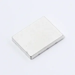
Certified shielding configurations designed for high reliability in medical electronics and smart devices.
View Details →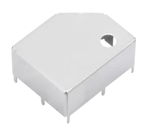
High-performance board-level shielding frames for automotive sensor applications.
View Details →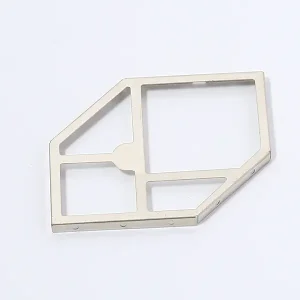
Integrated multi-compartment shielding frames for high-density IoT electronics.
View Details →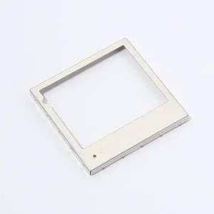
Nickel-alloy shielding frames designed for thermal and EMI protection in high-frequency applications.
View Details →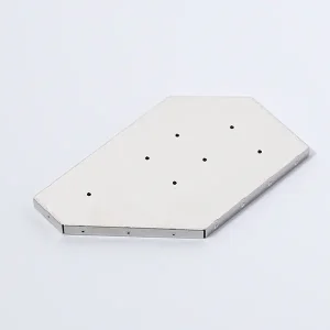
Precision stamped shielding components for high-reliability communications infrastructure.
View Details →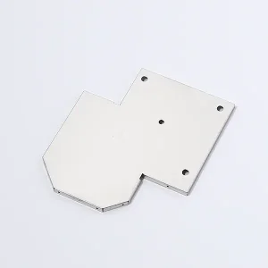
Custom shielding solutions engineered to maintain RF signal path isolation.
View Details →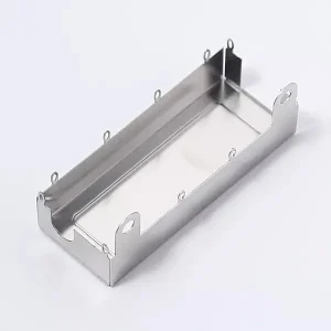
Durable, light-gauge metal shielding frames for low-profile consumer electronics.
View Details →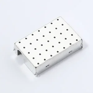
Engineered shielding frames designed for reliable solder contact on multi-layer PCBs.
View Details → Stpete Electronics