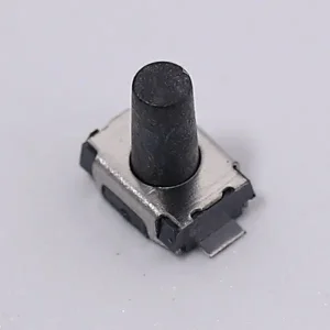
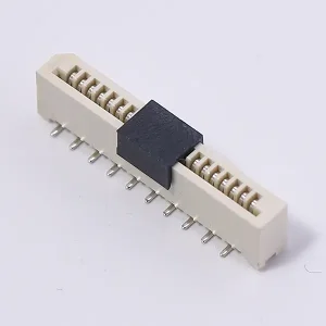
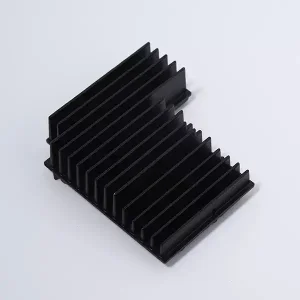
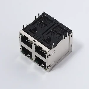
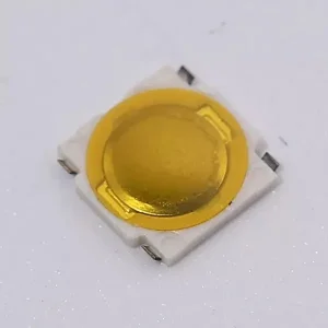
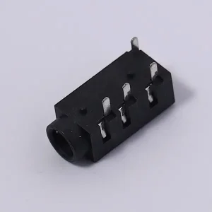
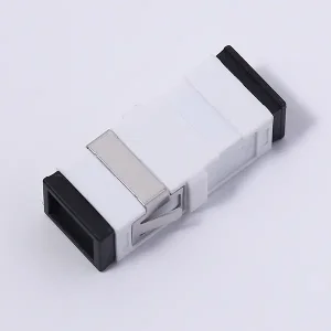
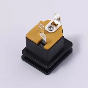
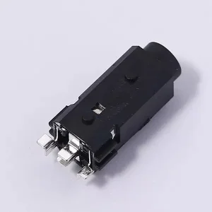
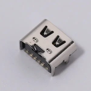
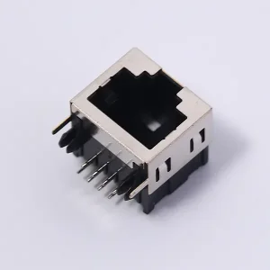
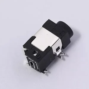
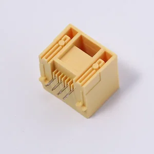
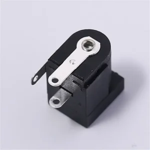
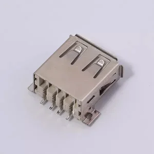
Explore our CE Certified electronic components and high-precision terminal configurations engineered for signal integrity.
Established in 2005 - Empowering the Electronics Supply Chain for 20+ Years
Wenzhou Stpete Electronics Technology CO., LTD is a certified high-tech enterprise specialized in the R&D, precision manufacturing, and international trade of advanced electronic connectors, radio frequency terminals, and customized shielding structures. With our extensive facility and direct proximity to global electronics hubs, we have built a long-term reputation among customers at home and abroad for excellent product quality, tight tolerances, and highly efficient trade services.
Our operation integrates high-speed stamping, insert molding, and automated assembly, providing turn-key components tailored to meet the strict electromagnetic compatibility (EMC) requirements of top global tech brands like Huawei and Hisense.

As electronic devices become faster, smaller, and more connected, protecting signals from EMI and RFI is paramount for performance and compliance.
Modern circuits operate at gigahertz frequencies, making them highly susceptible to electromagnetic interference (EMI) and radio-frequency interference (RFI). Without adequate shielding, adjacent high-frequency components—such as Type-C ports, RJ45 Ethernet connectors, and tactile switches—suffer from crosstalk, packet drops, or complete communication failure.
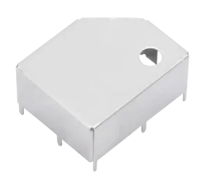
Board-level shields (BLS) act as mini Faraday cages, containing radiation at the source and preventing external noise from corrupting sensitive components. However, generic shields rarely fit the unique geometries and thermal limits of specialized PCBA layouts. This is where China Customized Shield Factories deliver decisive advantages through custom stamping, dynamic ventilation planning, and tailored multi-cavity designs.

China's manufacturing ecosystem combines unmatched scale, integrated raw material supply lines, and advanced machinery to offer high-velocity production at optimal cost points.
Equipped with high-level multi-stage progressive stamping presses and precision CNC centers. Progressive dies enable forming, piercing, and blanking at speeds up to 600 strokes per minute, assuring cost-efficient volume scaling.
We source certified copper alloys, brass, phosphor bronze, and stainless steels. Full trace analysis is provided with chemical composition certificates, complying perfectly with RoHS and REACH standards.
From component R&D (utilizing simulation tools like ANSYS HFSS for electromagnetic optimization) to physical tooling, high-precision stamping, surface plating, and automated tape-and-reel packaging.
The convergence of IoT, ADAS, and 5G/6G communication infrastructure is driving the evolution of advanced shielding designs.
As microprocessors push into the tens of GHz, traditional shielding methods face dimensional and thermal constraints. Several macro trends are reshaping how procurement managers and engineers source their components:
| Parameter | Standard Range |
|---|---|
| Available Materials | Nickel Silver, Stainless Steel, Phosphor Bronze, Brass |
| Material Thickness | 0.10 mm to 0.50 mm (Tolerances down to ±0.01 mm) |
| Shield Configuration | Single-piece (Fixed), Two-piece (Frame + Detachable Lid) |
| Plating Options | Tin (Sn) plating, Nickel (Ni) selective barrier, Gold (Au) flash |
| Packaging Method | Carrier Tape & Reel (EIA-481 compliant), Tray packaging |
Under Stpete Electronics, quality is always precious, guided by technology and based on safety.
Every step—from raw material selection to stamping processing, inspection, and packaging—is meticulously structured. Stpete Electronics operates in full compliance with international standards, holding certificates for ISO 9001 (Quality Management), ISO 14001 (Environmental Stewardship), and ISO 45001 / OHSAS 18001 (Occupational Health & Safety).
Our Quality Control lab operates advanced physical testing systems, including automated vision measurement systems (VMM), microhardness testers, plating thickness X-ray analyzers, salt spray chambers, and high-precision network analyzers for testing RF signal loss. This multi-gate inspection process ensures zero defect escapes to customer factories.
Our production floor features high-efficiency progressive stamping units, vertical and horizontal insert molding machinery, and bespoke high-speed automated assembly equipment. We continually introduce technological innovations to enhance our production capacity and accuracy.

Unity, cooperation, and continuous motivation underpins our long-term client success stories.
At Stpete Electronics, we strongly believe that technological innovation is fueled by collective team cohesion. To foster teamwork, communication, and mutual trust, our company regularly organizes team-building initiatives.
Whether overcoming challenges during technical R&D cycles or building alignment through outdoor workshops, our 200+ professional employees work collaboratively to solve customer problems. This strong cohesion translates directly into responsive client services, ensuring that custom design proposals and engineering questions receive comprehensive responses within a 24-hour turnaround.

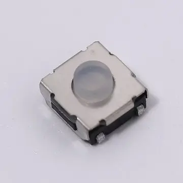
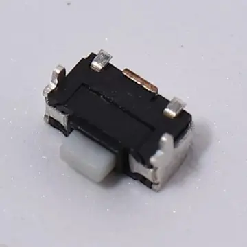
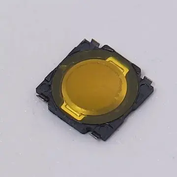
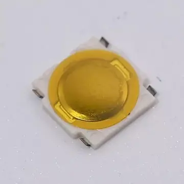
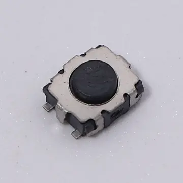
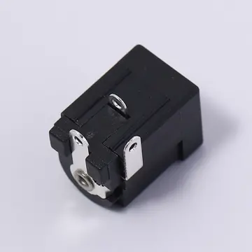
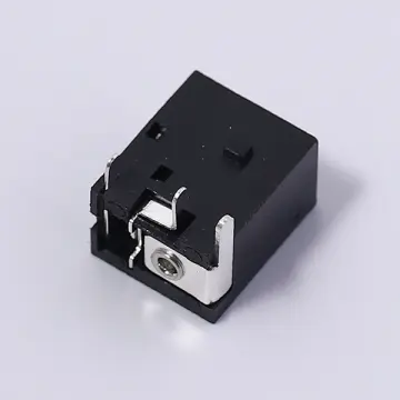
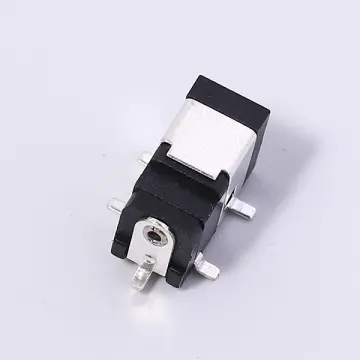
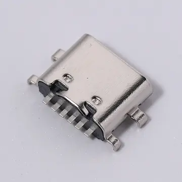
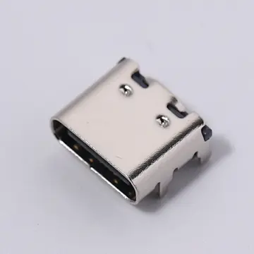
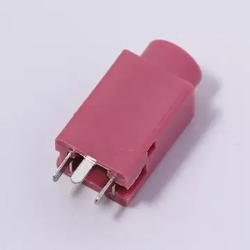
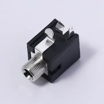
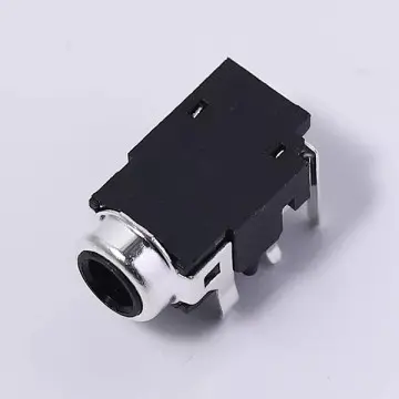
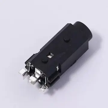
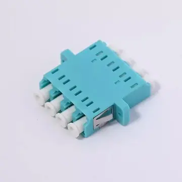
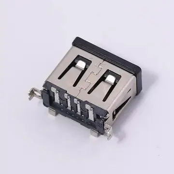
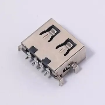
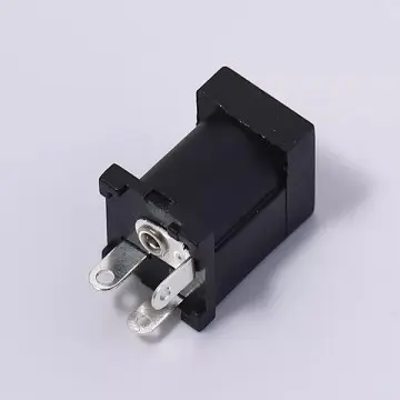
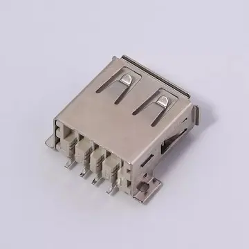
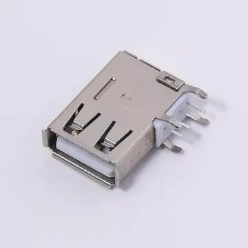
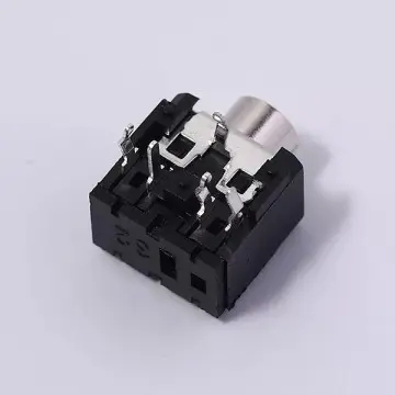
Original company components designed for advanced high-frequency circuits, telecommunications, and power distribution.
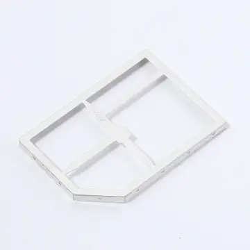
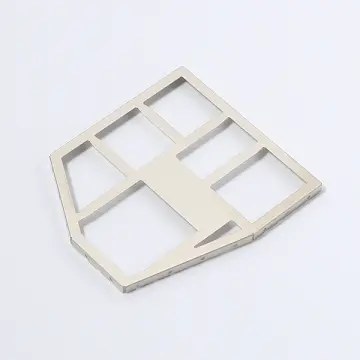
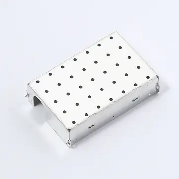
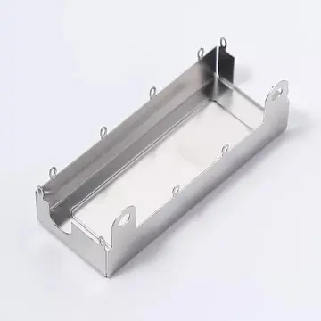
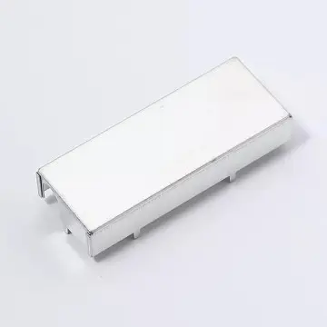
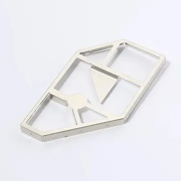
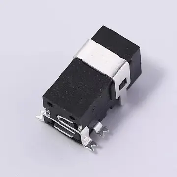
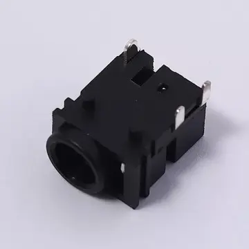
Technical answers to key procurement and engineering inquiries regarding customized shielding structures and connector production in China.
A: Nickel Silver (also known as copper-nickel-zinc alloy) is highly recommended for board-level shielding (BLS) because it offers excellent EMI attenuation, resists oxidation without additional plating, and is easy to solder during SMT assembly. For cost-effective solutions, tin-plated cold-rolled steel or stainless steel can be utilized, though they may require selective post-plating or specialized flux to ensure reliable solder connections.
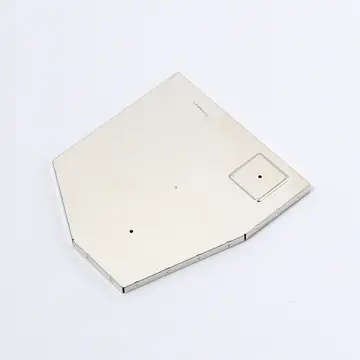
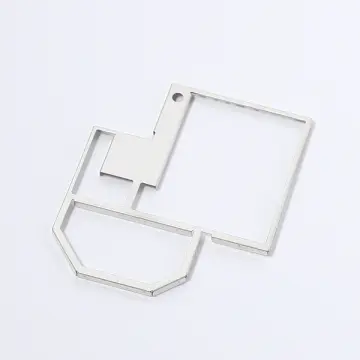
A: A single-piece shield is directly soldered onto the PCB, providing the most cost-efficient and structurally sound EMI barrier. However, it prevents access to internal components for repair or tuning. A two-piece design consists of a frame soldered to the board and a detachable lid that snaps onto the frame. This structure allows quick rework and component testing during development or after-sales servicing, though it incurs slightly higher tooling and unit costs.
A: We control coplanarity by using high-precision progressive dies and high-grade metal presses. Our automated optical inspection (AOI) systems check every batch, maintaining coplanarity tolerance to within 0.08mm. This precise planarity is essential to ensure that when the shield is placed on the solder paste during surface mount assembly, no gaps form that could compromise the electrical connection or allow EMI leaks.
A: Fast prototyping can be completed using laser cutting and soft tooling within 5 to 7 days, which is ideal for engineering validation. Once the design is locked, mass production progressive tool design and building takes 15 to 20 days, and manufacturing is executed rapidly, enabling us to ship volume orders within 2 to 3 weeks.
A: Yes, all products comply with CE, RoHS, and REACH directives. Our facility operates under ISO 9001 and ISO 14001 certifications. We perform strict raw material screening and provide full mill test certificates (MTC) and testing reports upon request to guarantee compliance for import markets in the US, Europe, and Japan.
For inquiries about our custom shielding solutions, connectors, or price lists, please leave us a message. Our technical sales team will contact you within 24 hours.
Get A Quote NowReliable component connections built for long-term endurance and signal protection.
 Stpete Electronics