Explore our premium product portfolio featuring customized plating, outstanding conductivity, and rigorous physical reliability certifications.
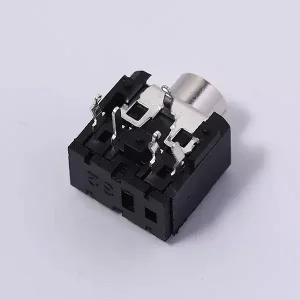
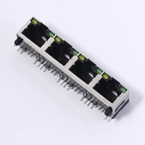
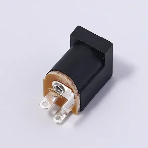
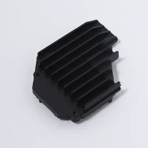

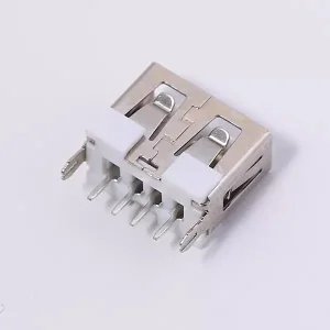
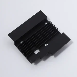
In high-frequency and critical micro-electronic assemblies, surface finishing is not merely a cosmetic step; it is the ultimate determinant of signal integrity, insertion resistance, wear longevity, and anti-oxidation metrics. As the global digital ecosystem transitions toward high-speed gigabit protocols (such as 5G/6G systems, USB 4.0, and advanced fiber networks), OEM plating suppliers must fulfill increasingly demanding micro-scale tolerances.
The global electroplating trend is shifting decisively towards sustainable, highly dense coatings. Advanced systems utilize selective gold/nickel deposit methods, precise localized tin overlays, and green chemical baths that significantly reduce heavy metal runoffs while preserving mechanical lifecycle ratings. Stpete Electronics utilizes proprietary electrolytic formulations to guarantee zero surface cracking and robust barrier resistance under long-term thermal loads.

A trusted high-tech pioneer established in 2005, serving global electronic supply chains with unmatched engineering rigor.
Wenzhou Stpete Electronics Technology Co., Ltd. specializes in the extensive R&D, advanced manufacturing, and strategic export of precision electronic connectors. Across two decades, we have constructed an international reputation for high-precision components, catering to Tier-1 telecommunication and consumer electronics brands including Huawei, Hisense, and other industry giants.
Addressing supply chain risks, signal decay, and material durability with localized support and world-class technology infrastructure.
Diffusion of copper substrate into outer gold/tin layers can degrade contact surface parameters. We apply a dense sulfamate nickel barrier to block copper migration, ensuring stable impedance and continuous data flow over 20+ years of usage.
By employing selective gold-flashing, hard gold overlays (up to 50 micro-inches), and cost-effective Palladium-Nickel (Pd-Ni) alloy configurations, our OEM connectors endure harsh environments and over 10,000 mating cycles without oxide build-up.
We solve cross-border supply hurdles via absolute adherence to RoHS 3.0, REACH, and Conflict-Free Mineral declarations. Through strategic logistical centers and reliable supply lines, we deliver JIT (Just-in-Time) shipments to Europe, APAC, and the Americas.
A deep-dive analysis of our advanced electroplating facilities, custom mold setups, and metallurgical laboratory validation.

Wenzhou Stpete Electronics operates fully equipped facilities housing high-speed automatic punching machines, precision CNC lathes, and automatic insert-molding assemblies. These machinery setups guarantee structural concentricity and precise pin dimensions for high-density components like Type-C connectors, network jacks, and needle assemblies.
To ensure perfect coating thickness and defect-free boundaries, our quality laboratories feature:
Our commitment to R&D is backed by an annual budget allocation of over 15 million RMB. Our engineering teams continuously pioneer customized plating formulations, such as low-whisker matte tin baths and lead-free alloy deposition methods. These developments prevent spontaneous tin whisker formation, a major cause of short circuits in automotive-grade electronic systems.
Collaborative designs with Huawei and Hisense validate our ability to implement highly sophisticated structures with complex localized patterns, saving material costs while boosting physical efficiency.

How Wenzhou Stpete Electronics coordinates engineering, assembly, and customer services to deliver reliable OEM solutions.
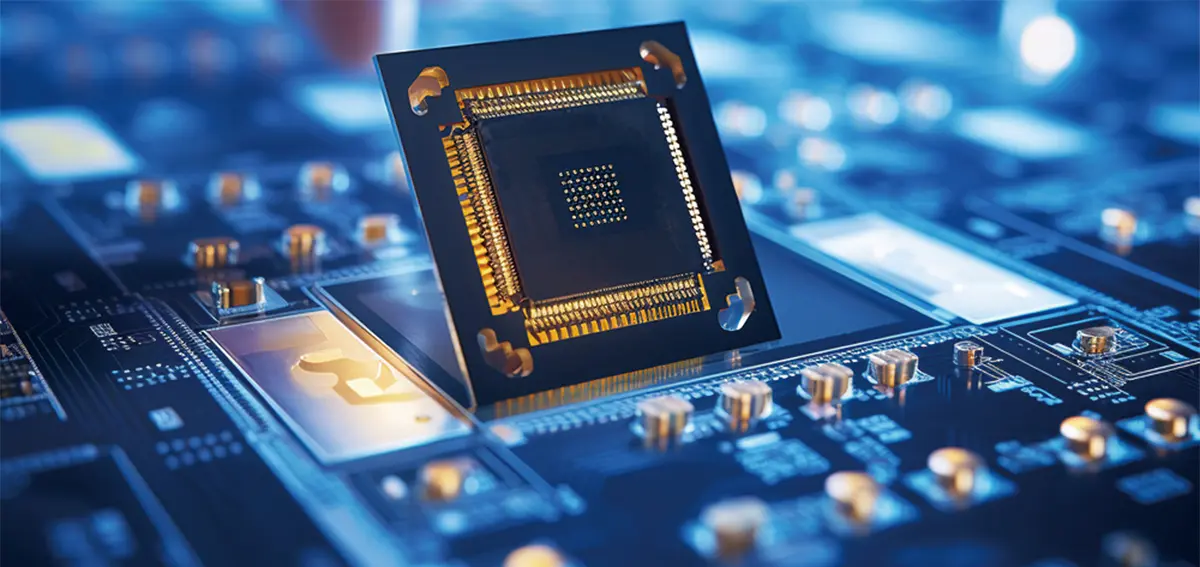
Our R&D team consists of more than 30 technical specialists focused on custom molds, dynamic signal models, and electro-chemical plating experiments. With 21+ patents and deep brand alignments, we quickly transform early drafts into manufacturing files.
Guided by safety and certified under ISO 9001, ISO 14001, and ISO 45001 standards, our inspection paths cover raw materials, initial punching runs, intermediate plating checks, and finished output tests.

Our insert molding, assembly, and automated testing routines integrate robotic systems to eliminate human assembly errors. This helps achieve near-zero defect rates (DPPM < 50) and meets rapid volume scaling goals.
Aligning with next-generation smart electronics, sustainable practices, and the clean manufacturing requirements of the 2030 decade.
As micro-electronic architectures advance toward 3D chip stacks and tight-pitch connectors (pitches < 0.5mm), traditional barrel and strip plating methods encounter operational limits. Stpete Electronics is developing advanced surface solutions to meet these emerging challenges:
This process confines high-velocity electrolyte jets to critical contact zones, reducing raw gold usage by 40% while ensuring uniform gold layer placement on contact crowns. This provides cost-effective gold coverage where it is needed most.
By blending tiny graphene sheets into our gold and silver plating baths, we produce composite surfaces with high wear life and excellent thermal stability. This enables contacts to endure higher current peaks without thermal degradation.
Wenzhou Stpete is replacing traditional cyanide-based gold plating chemistry with non-toxic, sulfite-based alternatives. This aligns with global ESG mandates and keeps our operations compliant with incoming eco-regulations.
Corporate Team Synergy: Outside the factory floor, Stpete promotes a culture of collaboration. Through annual team activities and ongoing technical training, we align our engineers, operators, and QC inspectors with one goal: delivering defect-free assemblies to our international clients.
Direct technical answers to common queries from global procurement managers and hardware design engineers.
Nickel serves as a physical barrier that prevents base copper from migrating to the outer gold or tin surface. Without it, copper atoms can diffuse to the exterior and oxidize, causing contact resistance to rise and compromising signal integrity.
We apply high-purity matte tin chemistry combined with a post-plating baking bake routine (typically 150°C for one hour). This relaxes the internal stresses within the tin crystal grid, suppressing the growth of whiskers that could cause electrical shorts.
We check coating thicknesses non-destructively using calibrated X-Ray Fluorescence (XRF) spectroscopy. To verify physical performance, we conduct mechanical cross-section analysis, solderability tests per J-STD-002, and salt spray exposure tests under ASTM B117 to guarantee corrosion protection.
Yes. Utilizing advanced strip-to-strip selective plating, we deposit gold only onto key contact zones while applying tin or nickel to solder tails. This lowers raw material costs while maintaining high connection performance.
Our manufacturing and electroplating processes are fully compliant with RoHS 3.0, REACH, and California Proposition 65. We offer complete material data declarations (IMDS/IPC-1752A) to verify the absence of hazardous substances.
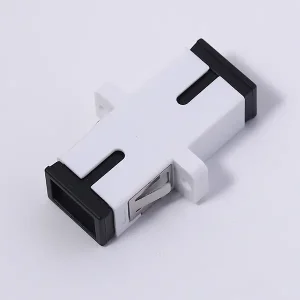
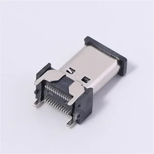
Explore our advanced range of fiber optic solutions, micro Needle connectors, and standardized USB interfaces built for demanding environments.
 Stpete Electronics