Engineered specifically to support modern high-speed SMT assembly in New England's high-tech manufacturing corridors.
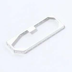
Optimized for low attenuation loss in biomedical and diagnostic sensing PCBs.
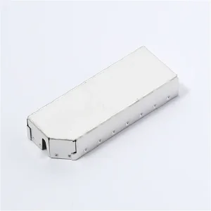
Engineered for rugged military-aerospace subsystems operating in complex RFI fields.
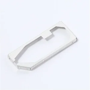
Ultra-flat baseline <0.08mm to minimize solder defects in micro-packaged assemblies.
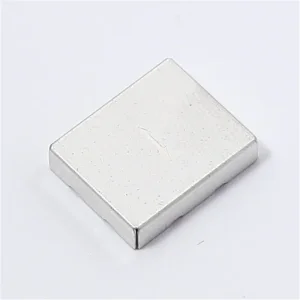
Corrosion-resistant custom alloys designed for harsh oceanographic electronics.
The Greater Boston area—including key technological corridors like Cambridge's Kendall Square, the Route 128 high-tech belt, and the Waltham defense hub—is one of the world's most demanding environments for electromagnetic compatibility (EMC). As home to world-leading biotechnology institutes, high-mobility robotics pioneers, and Tier-1 defense contractors, the local market leaves zero margin for signal interference.
Modern medical imaging tools, autonomous warehouse drone swarms, and advanced radar systems all rely on dense RF layouts. The integration of high-speed digital processors alongside highly sensitive analog transceivers makes board-level electromagnetic interference (EMI) a critical threat to system operation. Our high-precision shielding frames are designed to isolate key RF circuits, guaranteeing maximum performance under stringent FCC part 15 rules and military standards.
Through our dedicated supply chain, we act as a reliable offshore production partner, delivering custom-manufactured, CE-compliant shielding frames directly to prototype houses, SMT assembly plants, and systems integrators throughout New England.

Providing technical depth for hardware engineers working on demanding RF, microwave, and high-frequency digital designs.
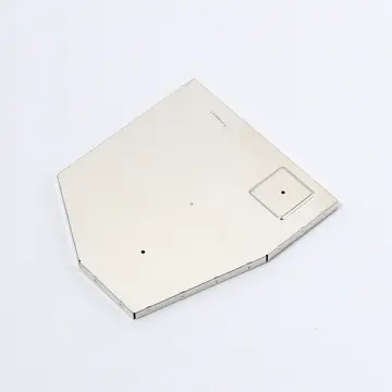
We work with high-quality Nickel-Silver (Cupronickel) and Tin-Plated Brass. Nickel-Silver is solderable, highly resistant to oxidation, and provides superior attenuation (up to 80dB in high-frequency regimes) without requiring subsequent plating operations.
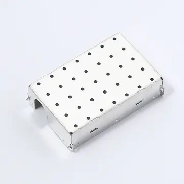
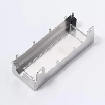
Our shielding frames feature calculated ventilation micro-hole patterns. These patterns maintain EMI attenuation integrity (ensuring hole diameters stay below λ/20 of the target frequency) while allowing heat dissipation and visual inspection of internal components during reflow.
Using advanced multi-stage progressive stamping and CNC flattening, we maintain strict coplanarity across large footprint shields. This prevents cold solder joints and gap leakage, optimizing automated SMT pick-and-place lines.

Established in 2005, Wenzhou Stpete Electronics Technology CO., LTD is a high-tech enterprise specialized in the development, production, and sales of electronic connectors and customized precision shielding frames. We have built an excellent reputation among customers at home and abroad for top-tier product quality and highly efficient trading services.
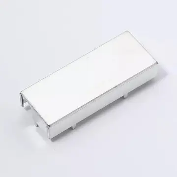
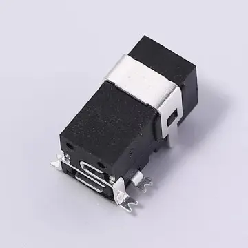
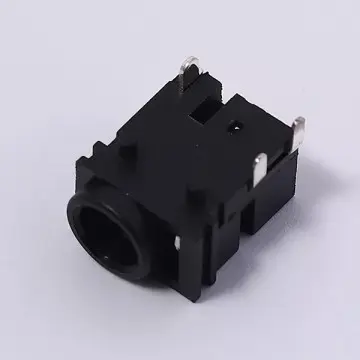
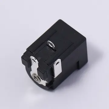
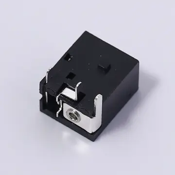
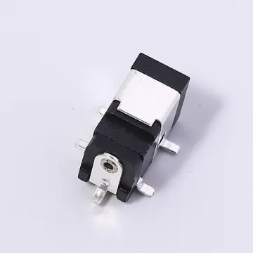
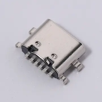
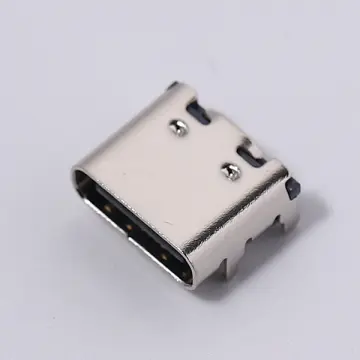
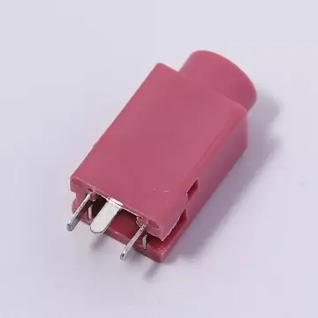
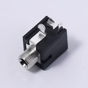
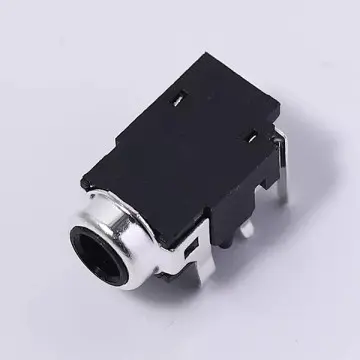
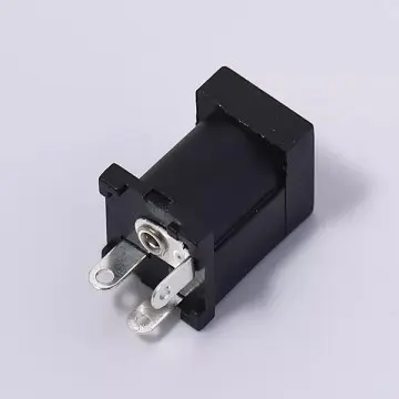
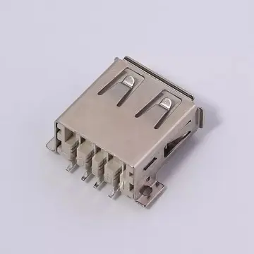
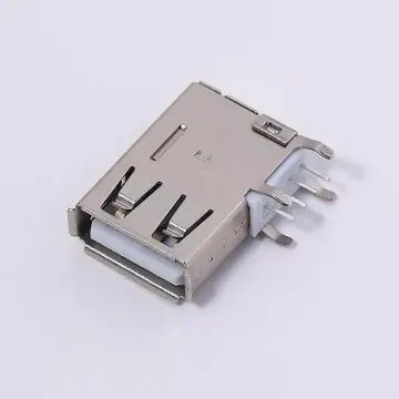
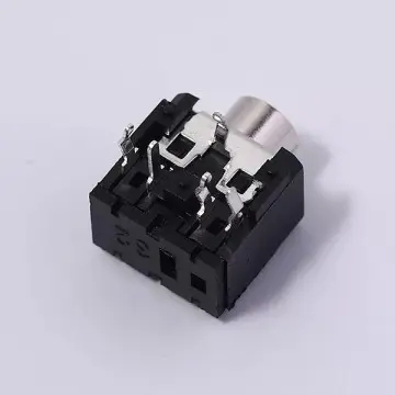
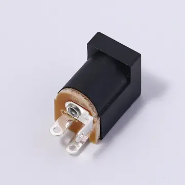
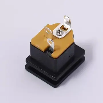
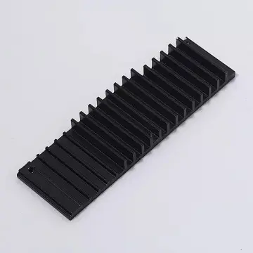
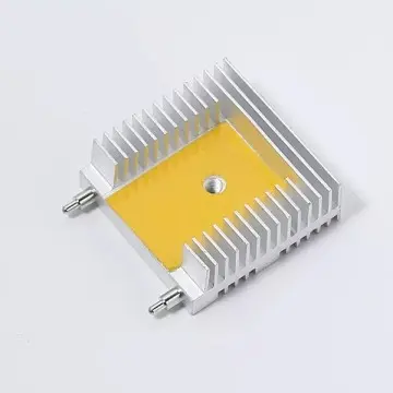
Our modern manufacturing facility is fully equipped to produce IF Radio-Frequency Terminals, FCB Network Jacks, DC Power Outlets, USB Sockets, AV Pin Jack Boards, Radiators, and custom metal shielding cans. Using high-level progressive stamping machinery and high-speed CNC machines, we ensure exceptional accuracy and reliability for every production batch.
With an experienced R&D team of over 30 technical personnel, we continuously collaborate with global technology giants and top domestic brands like Huawei and Hisense to push the boundaries of high-speed high-frequency signal integrity.
Every step in our production is meticulously audited to guarantee absolute reliability on the PCB board.
For Wenzhou Stpete Electronics, quality is our primary focus. We believe that technological innovation combined with strict process control is the ultimate driver for industrial growth. From the initial raw material sourcing (utilizing certified premium metals) to on-line processing and post-production tolerance validation, every step is carefully logged.
Our facility holds certifications for ISO 9001:2015, ISO 14001, and ISO 45001 (successor to 18001). We own over 21 research and development patents, illustrating our commitment to design innovation. To ensure zero-defect integration at our customers' plants in Boston and globally, we employ optical image inspection machines, precision flat-bed scanners, and network analyzers for real-world RF verification.
Our integrated capabilities in insert molding, complex finished product assembly, and highly automated production lines allow us to scale from low-volume prototypes to high-speed high-volume production without compromising tolerances.

How our shielding components address electromagnetic interference across key regional industries.
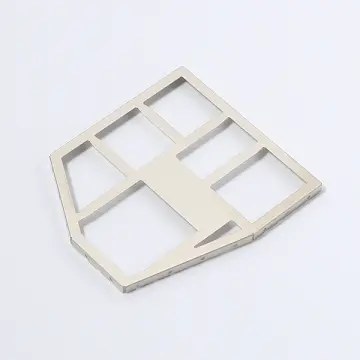
MRI components, point-of-care diagnostics, and patient monitoring wearables in Boston's hospital networks require exceptional signal integrity. Our multi-cavity shielding frames isolate sensitive pre-amplifier circuits from ambient high-frequency interference.
Warehousing and delivery robotics rely on high-frequency LiDAR, motor encoders, and RF communication modules. Our ruggedized, SMT-mountable frames block high-frequency switching noise from powerful DC motor drives, protecting sensor inputs.
Smart factories deploy multiple sensors communicating via Zigbee, LoRa, or Wi-Fi. Our cost-effective, custom tin-plated steel shielding cans provide excellent near-field magnetic attenuation, ensuring stable sensor node operation in electrically noisy environments.
Supporting developers and engineers through the transition to next-generation RF designs.
As communications advance toward 5G-Advanced and millimeter-wave (mmWave) 6G architectures, traditional shielding methods face limitations. Higher frequencies reduce electromagnetic wavelengths, making even microscopic physical apertures potential RF leak paths. Our engineering roadmap addresses these challenges through three key development tracks:
Fostering collaboration, communication, and technological progress.
We believe that strong internal teamwork leads directly to excellent customer service. To build unity and cooperation among our employees, Wenzhou Stpete Electronics organizes regular team-building activities, such as outdoor training programs.
These exercises encourage participants to step outside their comfort zones, build mutual trust, and develop creative problem-solving skills outside the typical office environment. This focus on collaboration helps reduce work-related stress, enhances overall morale, and drives our engineering and production teams to approach complex client requests with energy and focus.
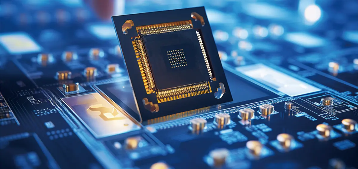
Answers to common design and sourcing questions from RF engineers and procurement specialists.
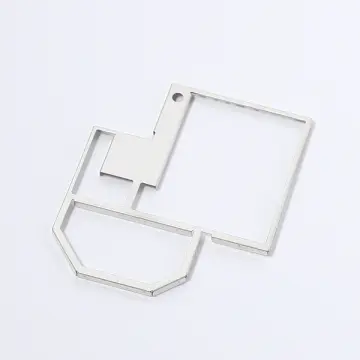
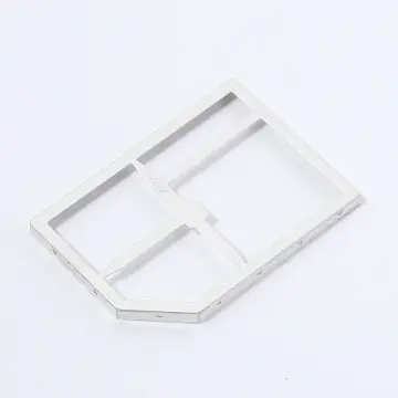
Select from our certified shielding designs configured for diverse industrial demands.
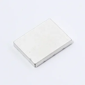
Designed for compliance with industrial and automotive electronic sub-assemblies.
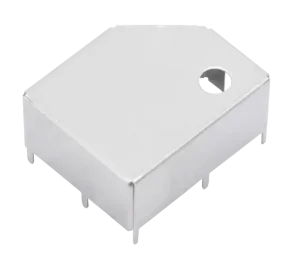
Optimized for high-density cellular and base station transceiver boards.
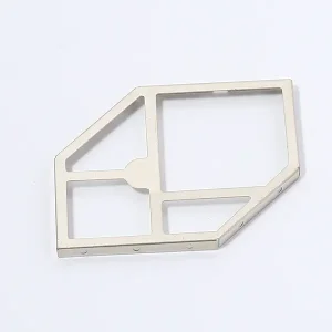
Provides low-leakage performance for sensitive imaging processing units.
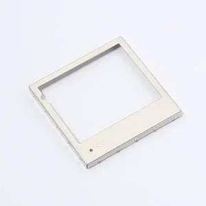
Engineered to protect low-noise analog circuits from digital switching noise.
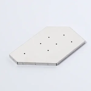
Featuring reinforced SMT contact feet for high-vibration robotic applications.
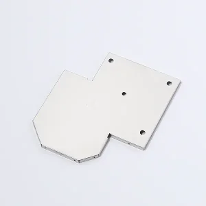
Designed for low attenuation loss in biomedical and diagnostic sensing PCBs.
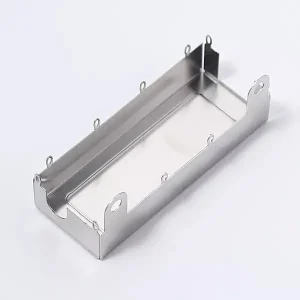
Allows separation of local oscillators and RF amplifiers under a single cover.
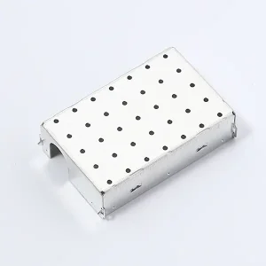
Specifically tuned to isolate Wi-Fi/Bluetooth signals from adjacent MCU buses.
We maintain a modern manufacturing footprint with advanced tooling and validation instrumentation.
Meticulous validation processes verify structural dimensions and coplanarity profiles before batch shipment.

High-speed progressive tooling handles high-volume runs with stable, repeatable dimensions.
Every batch of raw material is checked to guarantee standard solderability and mechanical strength.

 Stpete Electronics